KRN SEMI (KRNSEMI) was founded by former R&D engineers from the semiconductor industries of mainland China and Taiwan.
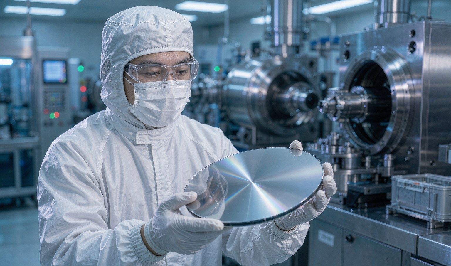
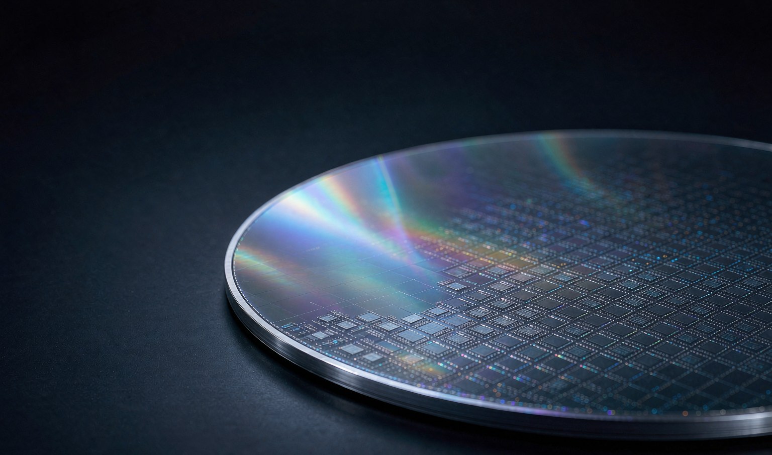
KRN designs, packages, tests and distributes ICs and discrete semiconductors, and specializes in the wafer-level design of power and protection devices.
For years we have combined R&D innovation with core technologies to serve industrial, automotive, consumer, communication, medical and computing markets. We focus on high-quality, high-performance analog ICs and power devices, always planning and developing against international benchmarks.
Serving customers worldwide is the KRN principle. Ownership and management are clearly separated, professional managers are engaged, and operations are institutionalized for the long run.
Capital broad-based, ownership clearly separated from management; professional managers engaged to improve performance; institutionalized operations aimed at sustainability.
Former R&D department of the Taiwanese semiconductor industry; technical leadership with 15+ years, core members with 10+ years of design experience.
Taiwanese semiconductor technology with in-house wafer design; TSMC 8-inch VD-MOS platform; long-term assembly partners including JCET.
Over the years KRN has become a long-term partner of automotive electronics suppliers, consumer electronics brands and EMS companies.
ISO 9001 compliant, with strict inspection at every production step to deliver consistent product quality.
Technical support and customization: cross-reference, parameter tuning, package customization and failure analysis, engineer to engineer.
No leaps in our story — just one line after another, one series after another.
KRN was established by former R&D engineers from both sides of the strait, starting from wafer design of power and protection devices. The first packaged series — DFN1006-2, DFN0603 and DFN2510 ESD protection diodes — entered the market the same year.
Adopted the TSMC 8-inch VD-MOS platform, building a complete development path from epitaxy to wafer, and obtained ISO 9001, ISO 14001 and ISO 18001 certification.
One epitaxy plant, two wafer fabs and two assembly plants came into place, closing the loop from design to shipment, with long-term partners including JCET.
Beyond MOSFETs, diodes and ESD, we added power management, amplifiers, interface, sensors and converters — now 11 product families and 4,002 part numbers.
Inductor lines run under the same semiconductor-grade quality system: molded, multilayer, magnetic glue and common mode, covering 0402 to 1210.
Inspection finds defects; it does not build good parts. We move control points upstream to incoming material, process parameters and equipment condition.
Incoming, in-process and outgoing control; critical steps have check points that trigger review on drift.
Chemicals and waste managed under the system, meeting customer audits and export requirements.
Working environment and personal protection institutionalized for stable output and delivery continuity.
Inspection data shipped with every lot: electricals, appearance, solderability — traceable to the lot.
Our Hsinchu R&D center and the Shenzhen sales and support team can arrange a call or a factory visit anytime.